What started out as a very misfortuned PC based off an AIR 486SH motherboard, a 66MHz Intel i486DX2 processor, and 8 MB of RAM, traveled a very bumpy road, fell off a cliff once or twice and managed to clamor its way back up somehow, and eventually became something much stronger!
For my latest PC restoration project, I found listed a PCchips M748LMRT, a very strange kind of motherboard with not just a purple AT keyboard connector, but both Socket 370 and Slot 1 on the same motherboard! This board is made to take either-or, and this is possible because the two sockets are very closely related (hence, the ‘slotket’ adapters existed – this board basically has one built-in).
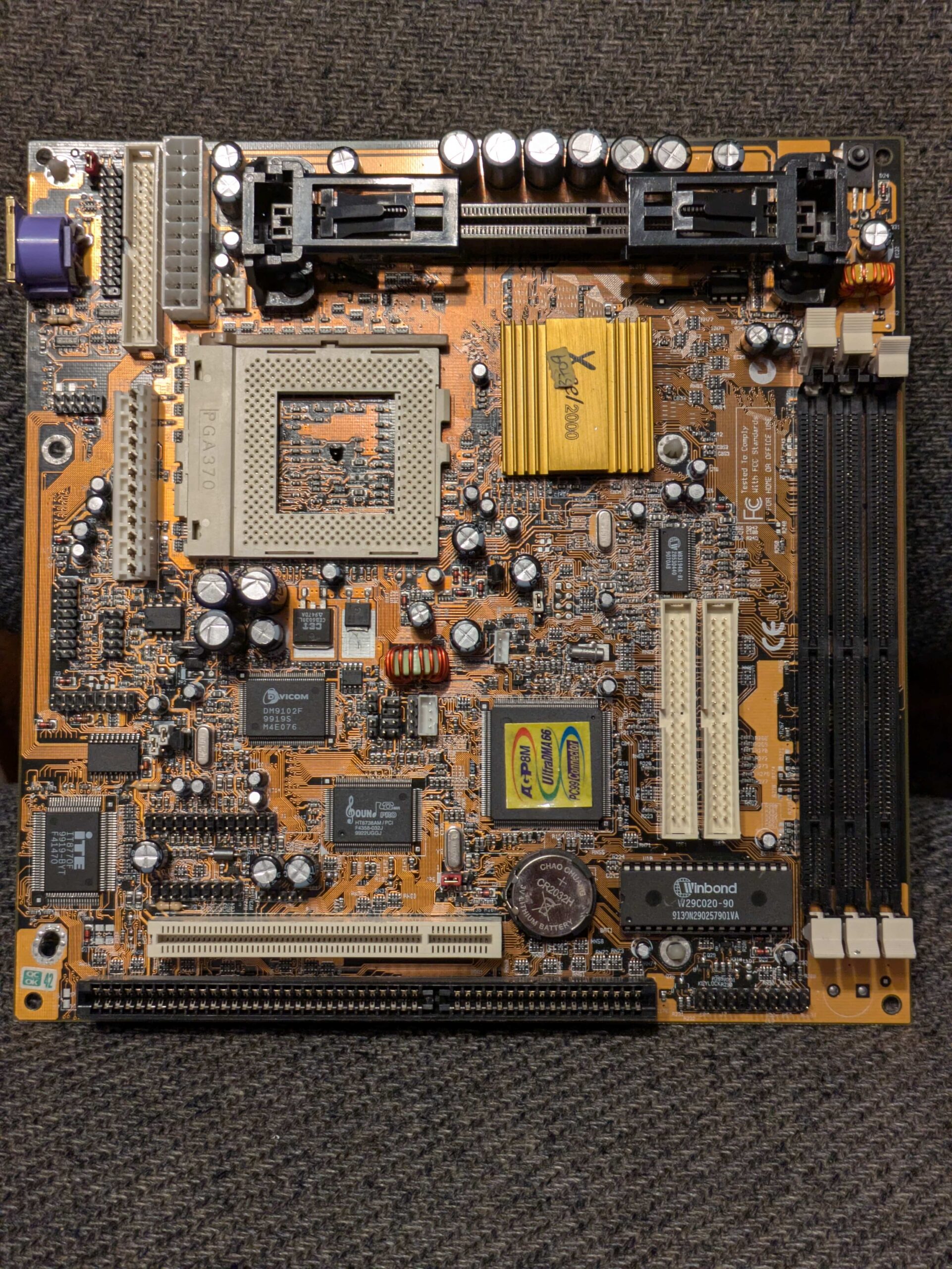
This board was described by the seller as getting stuck at the BIOS text: “Checking NVRAM...,” which according to this Twitter post, means it’s likely the BIOS chip is failing. I decided I’d pull the trigger on it – it’s easy enough to replace that.
I got the board in, and it turns out I wasn’t having that problem! Nice! But I’m still suspicious that the BIOS chip is likely failing, and sure enough, updating the BIOS bricked the board. I tried to update because I wanted to see if it’d let it accept the Coppermine-128 architecture Celeron I had sitting around, which it turns out this board doesn’t at all support anyway.
BIOS, Sockets, and Processors! Oh my!
Okay, bricked board? Sure, great, that’s about what I was expecting to happen anyway.
The original is an ASD AE29F2008-12, which considering I’ve not heard of that brand until now, I’d imagine isn’t the highest of quality. Thankfully, the Winbond W29C020-12 uses the same DA 45 identification code as the ASD, so it seems like a great replacement candidate. So, I ordered away!
I receive the Winbond, program it, and yep, it works! Great, the board boots now. And then I go and order a very cheap Socket 370 500MHz Celeron to really max this board out!
It was at this point I found out that putting any CPU in Socket 370 would get stuck at the NVRAM check, yet the Slot 1 266MHz Pentium II I was using wouldn’t trigger this. Blast it! I guess the Socket 370 is screwed somehow. So I used a slotket adapter, which as silly and redundant as that felt, wound up working with the Celeron perfectly fine. At least there’s that!
Oh, but I then remembered I had a good old Slot 1 Celeron 300A sitting around! I dug that up, put it in, and after putting a heatsink onto it with a ziptie, it worked perfect! And then I did the famous 66>100MHz FSB overclock, getting it to a whopping 450 MHz! Wow!
Well, that can’t be good…
The fun didn’t last very long. I booted up my Windows 98 SE installation, got a text-based error message, then smelled some smoke. After that, the board wouldn’t boot up anymore! Oh CRAP!!
This was the sign I had opened the portal to PCchips hell. I was scratching my head – what died? I didn’t see any obvious damage, even scrutinizing the board carefully. I just couldn’t see any evidence of any burnt components, on top of the bewilderment of how an overclock could cause this. Sadly, I know all too well that smell of electrical smoke, so there’s no mistake about what happened, especially since the board doesn’t POST anymore. It just runs the fans, and strangely, the IDE hard drive doesn’t spin up either. It does if unplugging the ribbon cable, but not when plugged into the motherboard.
I thought that maybe with some kind of hope, perhaps my second BIOS chip died. Sure enough, I got verification errors when trying to reflash! Erasure is no longer working, just like the original chip. Maybe the BIOS failed, and that’s all?
Alas, even after a well-priced order of more Winbond chips, followed by a good write & verify, this did not make any difference for the board. So, now what?
Well, I went and really scrutinized the heck out of the board. This will be a continued theme – a lot of close looks followed. At one point, I felt something really hot! Ouch! There’s a very hot three-pin SMD transistor, designated Q31, hanging out at the corner of the motherboard. That sure can’t be right! There must be something going on here.
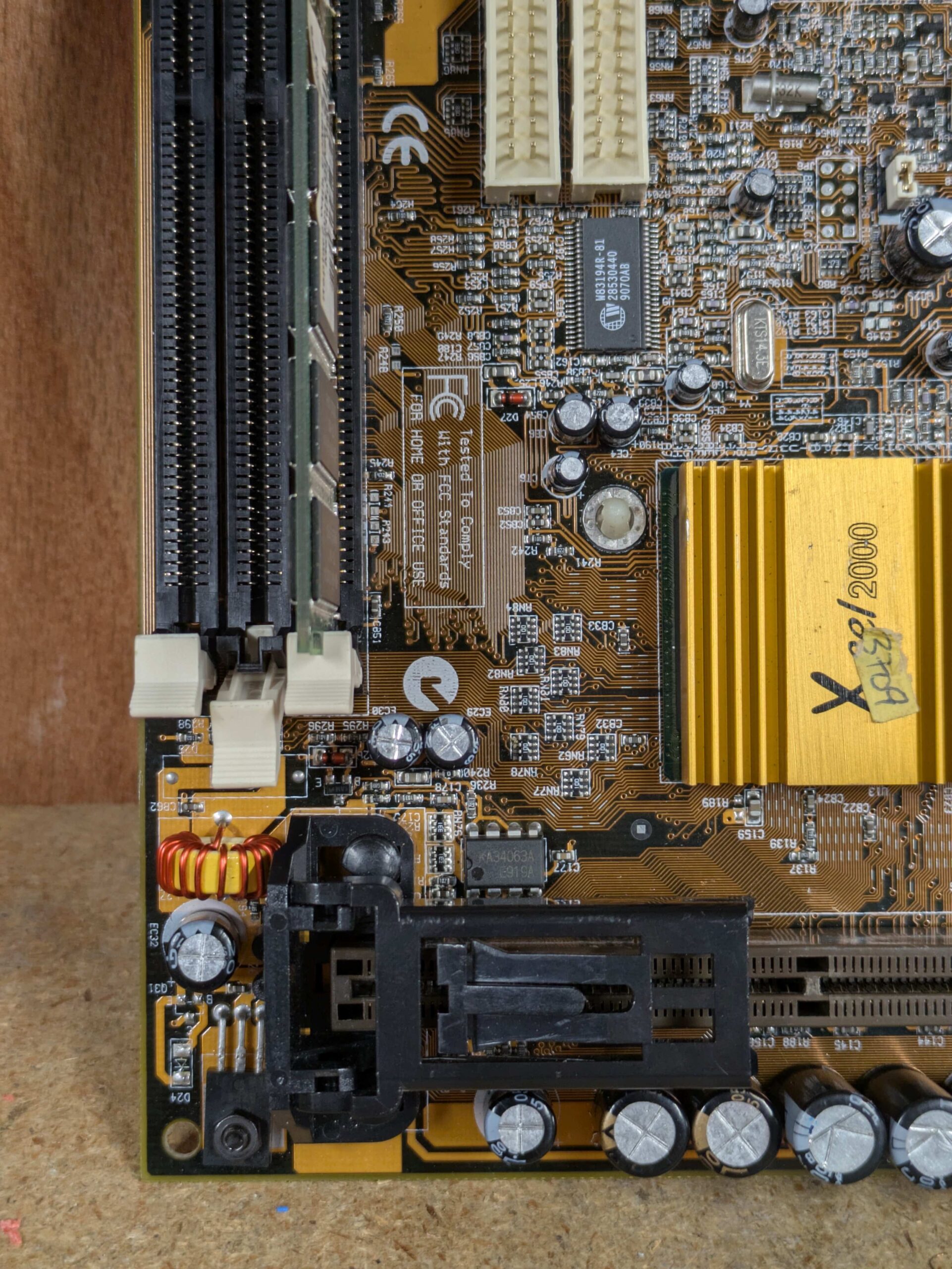
From here onwards came a whole lot of probing of the board. I really didn’t know much of what to make of it, so this is in fact where I chose to use ChatGPT to try and glean information about where to look and what to do.
Keep in mind that I do NOT treat ChatGPT like it knows everything – that’s a big mistake, and that’s where I roll my eyes and sigh about how many people misuse LLMs. It’s a database search engine – it has all knowledge, but zero wisdom, and specifics for every scenario will vary wildly.
So to use it properly, I think up questions and ideas to try, and give it measurements, so as to build an idea of what I’m looking at. I would probe things, give it what I saw, so on so forth, ad nauseam. I consider it like having another person that’s in the room, who might know a lot in general, but that I know more of the very specifics of the item I have in front of me.
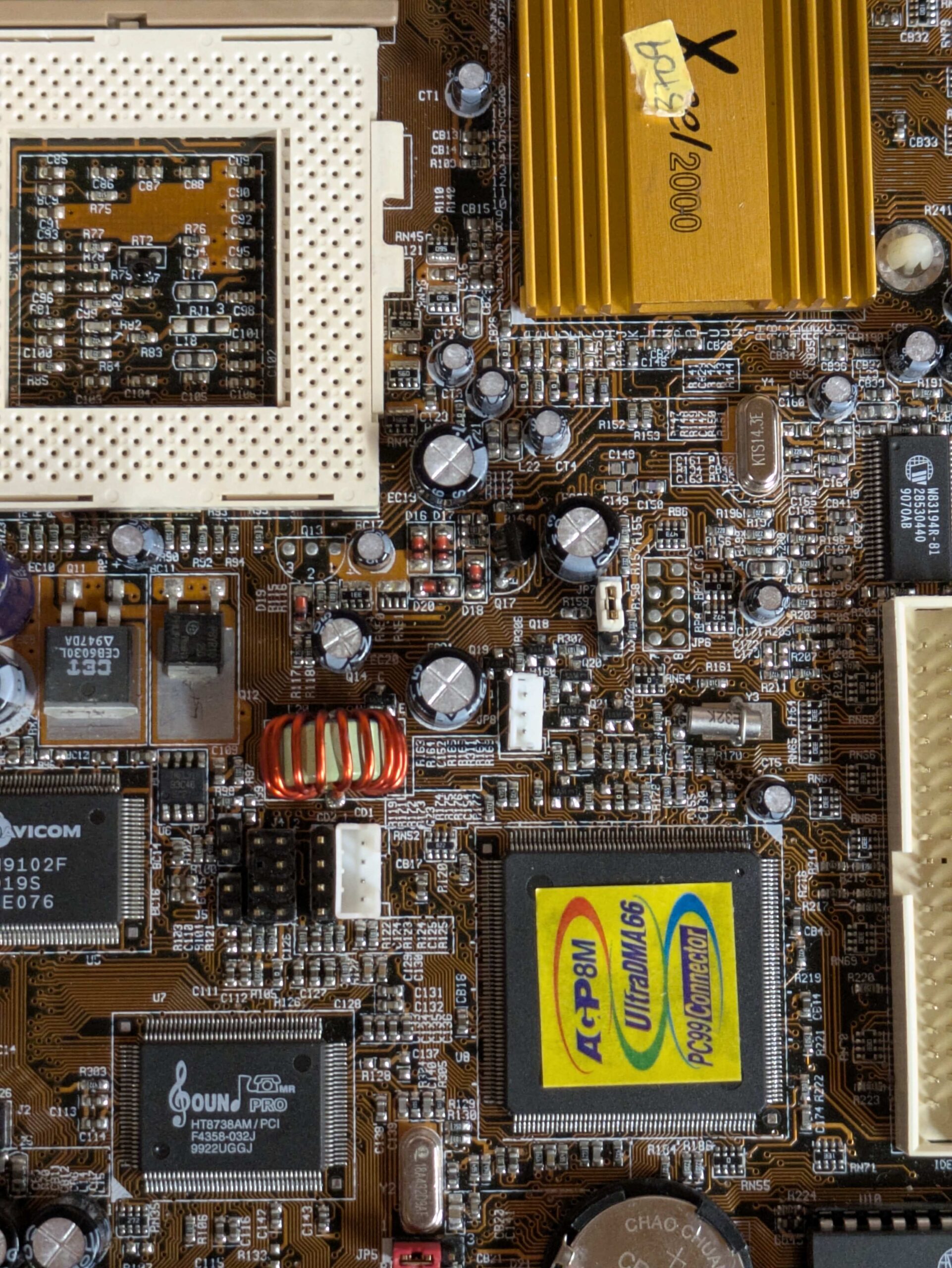
As quite an arduous mission, I had to take a lot of time away from it, and work at it in increments. I really didn’t know if this was going to have any hope at all. This is a cheap board, quite likely held together with duct tape, hopes and dreams. There’s no datasheet. No troubleshooting information to be found online.
Hell, it doesn’t even seem to have any beep codes, so whatever the reason it won’t POST, it’s not going to bother trying to tell you, even if it’s just your RAM that’s bad. The entire thing could be toast, the chipset having smoked itself to death, or it could even be the fault of some microscopic SMD component that I’m simply never going to find, leaving only wasted time, money, and effort.
The only little optimism carrying me through is that if it was a very nasty failure, that it’d likely leave some kind of visual evidence, even if subtle. That, and it’s still strange how it’d fail like this with an overclock – but granted, this is a PCchips board, so who really knows. Time will tell.
Cornering the Culprit
After much, much poking around and trying to get somewhere, I had discovered:
- The SDRAM has no +3.3V power!
- CPU Vcc is also missing
- Lots of power rails near the chipset are also dead
- Being an AT/ATX-powered board, the 3.3V rail is ignored entirely, and generated internally via two KA34063A DC-DC converter chips
- All these rails and many areas overall are only showing 0.86V when powered – not enough voltage to do anything
Eventually, after a number of days, I finally found the real answer – it really was the big transistor in the corner all along!! It was an NEC 2SD2583 NPN transistor, which now has turned into a dead short between pins 2 and 3. Although I had probed those pins and noticed continuity, I admittedly didn’t think much of it, as I had thought perhaps it was supposed to be a bridge.
Pulling that transistor out and using my multimeter confirmed that this is indeed a failed component. No wonder this is all happening! And so, its tiny neighbor Q31 was feeling the effects of this.
Well, now I’d like to make sure I know the rest of the board is good. Before I order any parts, I’ll try a Hitachi 2SC4242 NPN transistor, one I had ordered for a project some time ago and put aside. It’s not well-specced for the job, but maybe it could show something for us.
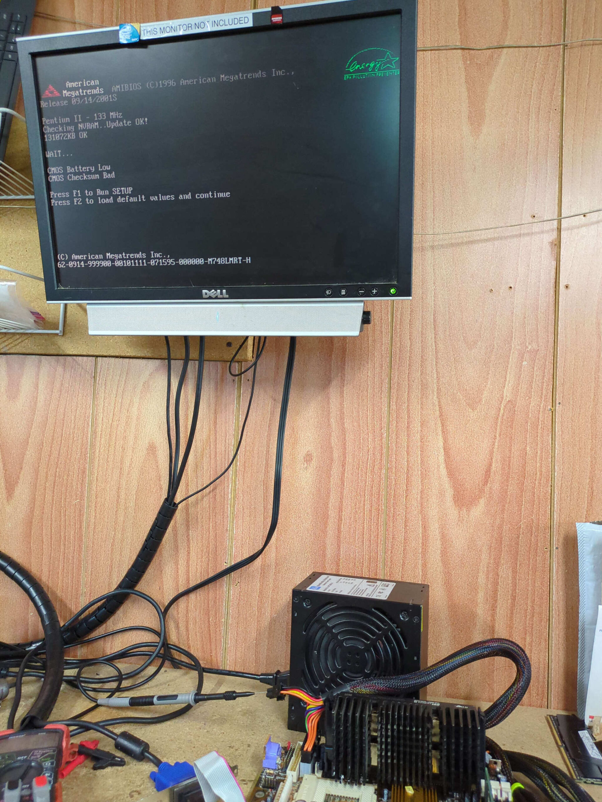
YES!!! IT LIVES!! Hooray!! What an incredibly wonderful plot twist! Quite interestingly, it seems the NVRAM check freeze is gone for any CPU used now. Perhaps that was the transistor failing the entire time! That’s incredible!
The original NEC 2SD2583 transistor is a low-voltage, high-gain component, whereas the Hitachi 2SC4242 is a high-voltage, low-gain component, more suited for a power supply than a computer motherboard. (It did indeed come from a power supply.) For this reason, it gets very hot after only a few seconds of running. But what matters here is, it proves that the board is alive!!
The NEC 2SD2583 is quite hard to find, and I didn’t have much luck searching thru my scrap motherboards either. After some research, I found the Sanyo 2SD1685-F to be a promising substitute, with much more suitable spec sheet for this application. So, I went and ordered those, and I waited.
The Recap
Before the new part comes in though, I’d like to treat this motherboard to a recap, to really prolong its life! A good tech buddy of mine has a bunch of brand new capacitors with perfect values to use on this motherboard, so I went to him and installed a bunch of those.
Unfortunately however, I forgot my preferred desoldering pump, and only had with me a cheap desoldering iron. I simply went with what I had, and it turns out that due to the tool’s recoil, I broke a few traces on the back of the motherboard! Arrgh! They’re thin, brittle and cheap on this board. It’s nasty. And the board no longer POSTs. Damn, it! Not POST-less purgatory again!
I will admit that it’s a pretty silly slipup on my part. But instead of throwing my hands up about it, I decided I’d use it as yet another learning opportunity along the way, and with some effort, I repaired the traces! I then put UV solder mask on top, to make it invulnerable. I was cautiously optimistic, since I had a good idea of which areas had suffered, and if I could track them all down, there’s a pretty good chance it should come back to life.
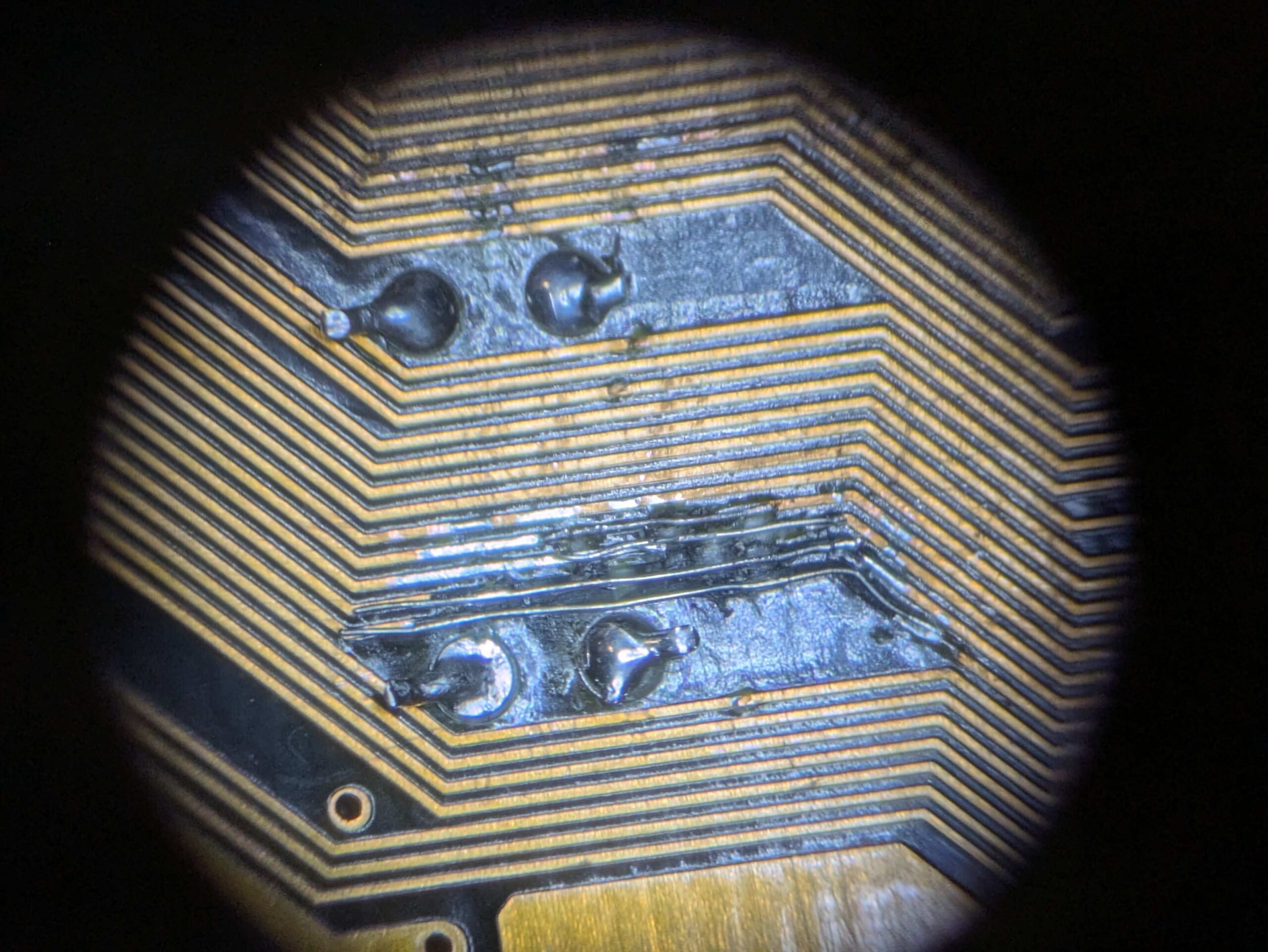
There were these traces, as well as one more that I needed to tend to. Miraculously, after doing this, it is working once more! Woohoo!! We’re back again! Now once I have the Sanyo transistor in, I can make this a finalized repair!
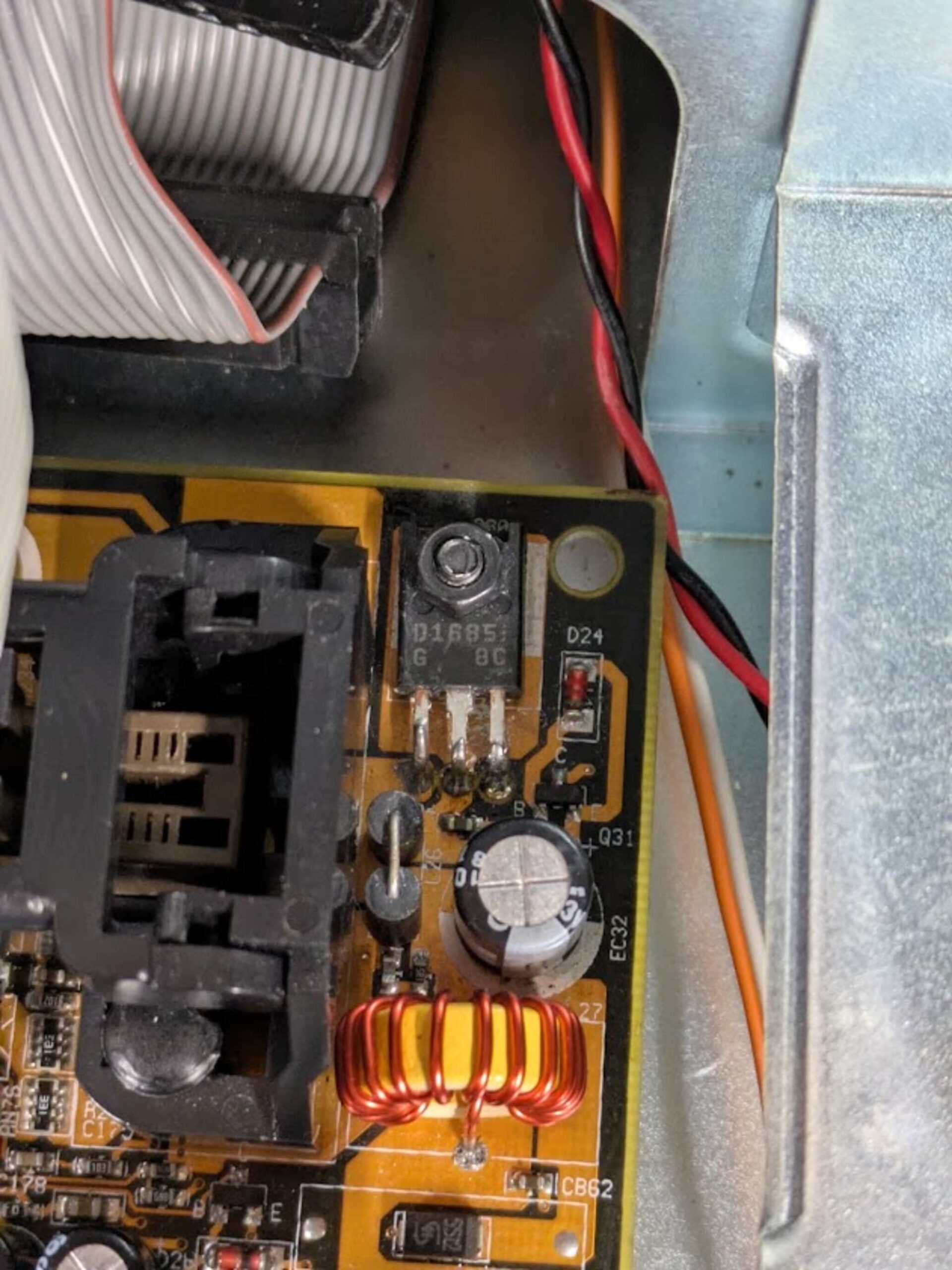
And here it is, installed! And sure enough, the board is working great now! Huzzah!! I put some thermal paste behind the transistor, to help conduct heat out of it and into the PCB. There was originally nothing there, and PCchips expected the pressure of the screw mounting to suffice. I doubt that any of this was well thought-out!
With hours of Memtest going, I can definitely feel the heat conducting well into the PCB. I call this a success! And thanks to the fact the CPU in the Socket 370 works now, I’m going to be using it with a 500MHz Celeron, and won’t bother with overclocking the 300A. This is easier on the motherboard, and in fact faster. So, a big win!
I also wound up reusing a couple of the original filter capacitors for the topmost area, in the spots where no capacitors were installed before. Only four of the spots were populated with 1500uF capacitors originally, and I kept the best-measuring originals for the remaining two spots. So, it gets upgraded filtering that it didn’t have from the factory!
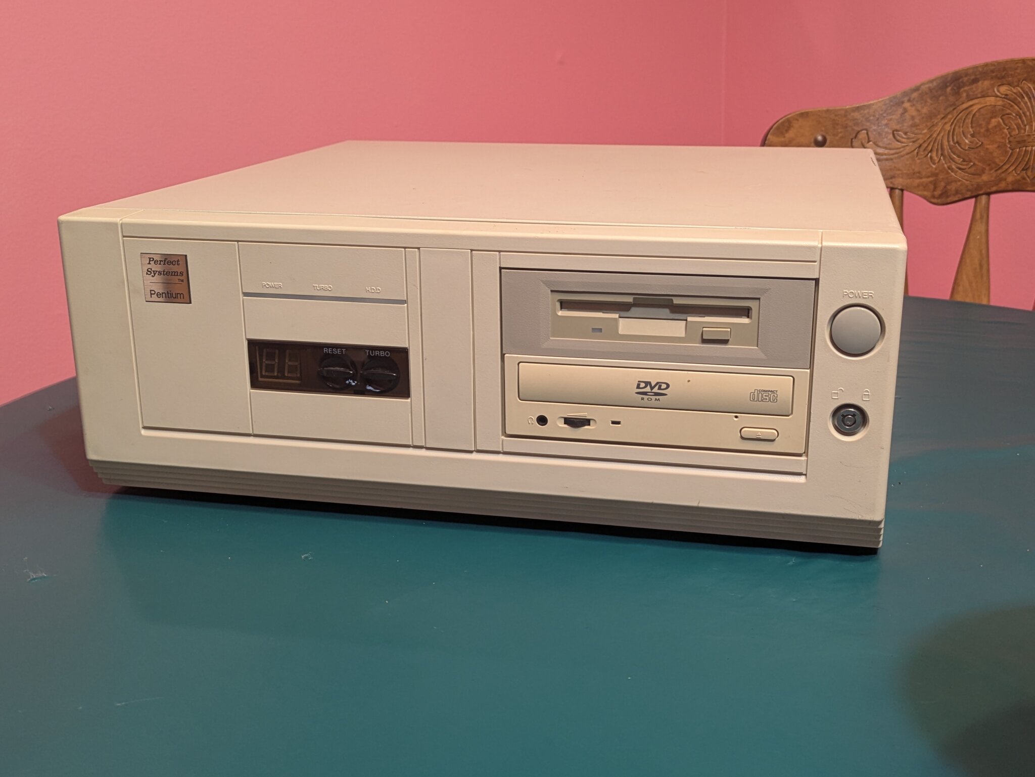
Pin Mappings §
Another very strange quirk of this motherboard is that it uses expansion slot brackets to house all the I/O. Seemingly, this is necessary due to the unusual combination of high integration in an AT motherboard form factor. As far as I know, almost no motherboards adhering to a proper AT standard feature onboard video & audio – yet this one does!
I’m lucky enough to have most of the original brackets! However, doing some searching on this board, not everybody is. So, I’d like to share the pin mappings, in case it can help anyone! (Do note that these are WIP, at the time of this writing, so more is to come.)
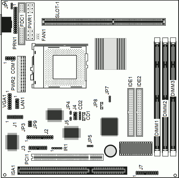
Pin mappings – click to expand
Other Facts §
Video Output Behavior
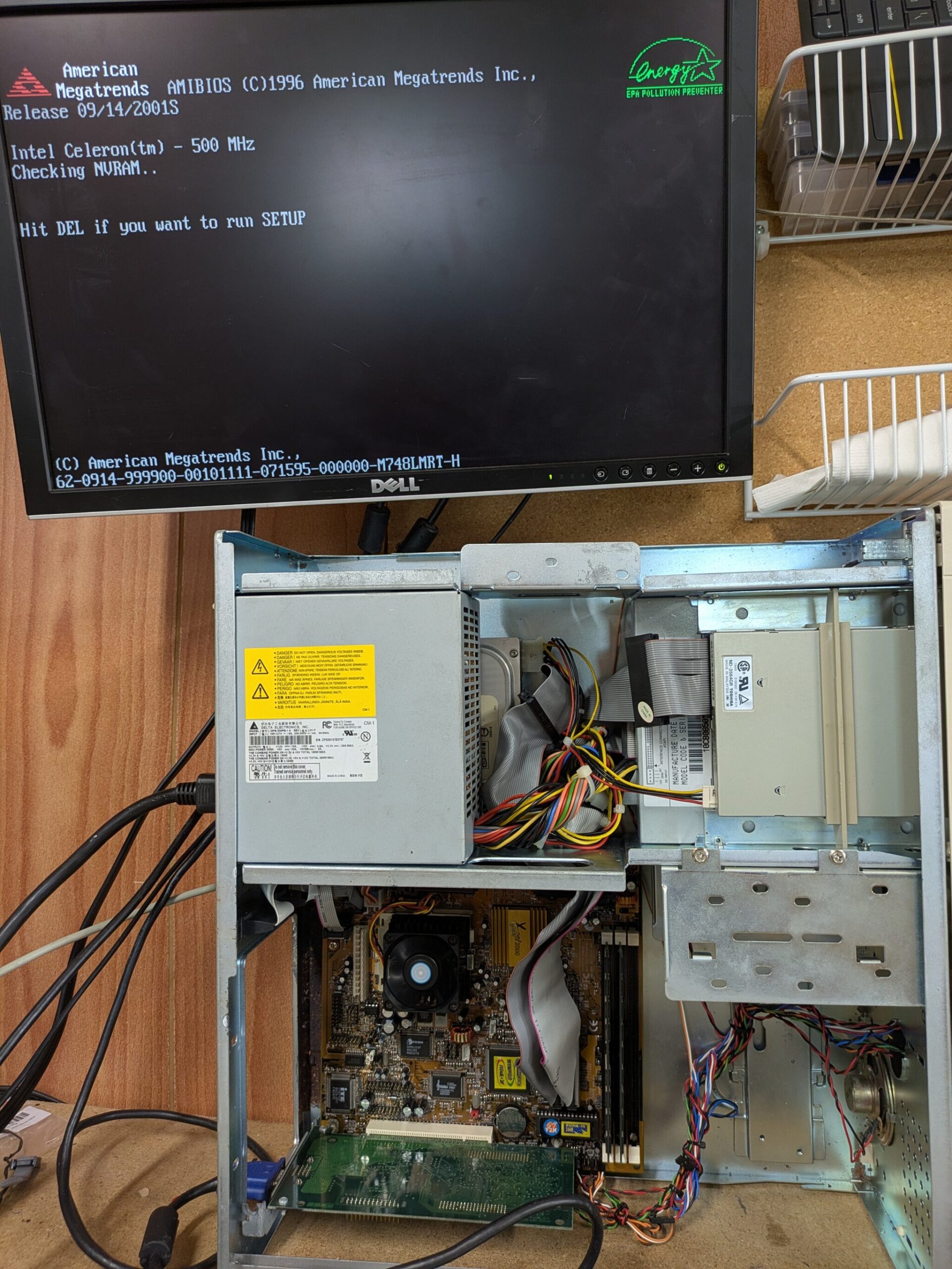
And on one more note, a thread on VOGONS.org mentions some trouble with getting a PCI video card to display. I’d just like to post this image here to show that at the very least, with my motherboard and a Compaq 296684-001 PCI card with an S3 ViRGE/GX 86C385 chipset, that it’s displaying no problem! PCI is the default video output in the BIOS, so after a CMOS reset, it will try to output over that first.
Informational Tidbits
- As above – PCI output is default, so if you lack the correct bracket, you can use a PCI video card (at least with 9/14/2001 BIOS)
- JP7 toggles whether Slot 1 (topmost two pins) or Socket 370 (lower two pins) will be used
- Yet funny enough, as far as I can tell, either socket works no matter what setting you use (at least with 9/14/2001 BIOS)
- CMOS doesn’t need to be reset when switching CPU sockets – it will tell you if it sees this happen
- Don’t put CPUs in both sockets – heaven only knows what’ll happen!
- Inductor L20 area (near Socket 370) is where Vcore is generated for all CPUs – this is the VRM
- Inductor L27 area (right of Slot 1) is where I/O voltage is generated, for use by the chipset, SDRAM, and the selection logic for Vcore
One more tip: don’t do what I did and accidentally slip your multimeter probe between pins 1 and 2 of Q11 near L20, even if for a split second. 5V into Vcore = POOF goes the processor! Whoops! Thankfully, the board is fine.